
I’ve often seen it said online that the LM13700 is just two CA3080’s in one package. Even by one of the co-designers! While it’s almost true, it’s not exactly right, and the little differences are sometimes important, so I thought we could take a look at what the differences are. Luckily we have schematic diagrams for the chips in the datasheet. While they’re not absolutely 100% accurate (they’ve been simplified in some respects), they provide enough information for us to see what’s going on.
A crash course in current mirrors
Firstly, we need to be able to recognize some of the functional blocks we’re going to see. I was learning electronics in the era when the 741 op-amp was everywhere, so I’m pretty good with op-amp circuits and can recognize the usual designs. Transistors however are a different story and I’m not half so comfortable with transistor circuits. So bear with me while I get up to speed!
There’s not much you need to know about transistors to understand an OTA in truth. The building blocks are basically a differential pair for the input (the “Long tailed pair”) fed by current mirrors. We do need to take a look at a couple of current mirrors though, so let’s do that first.
The simplest current mirror – the Widlar mirror
This is about as simple as a current mirror can possibly get. It’s two transistors base-to-base, and one has its base tied to its collector. This is known as a “diode-connected transistor” because one of the NP junctions is effectively shorted out, so what remains is the other PN junction – a diode.

On the left is the actual circuit, and on the right is the equivalent circuit with the diode-connected transistor replaced by a diode. This is commonly done in the internal schematics you see in OTA datasheets, so it’s important recognize it drawn this way, but also to know that what’s really going on is the situation on the left.
So what does it actually do? Well, if we connect a resistor to some voltage and feed in a current Iin at the top-left, it “mirrors” that current into the connection at the top-right, Ic. How does this work?
As long as the voltage at Q1 collector is higher than the forward voltage of the base-emitter junction (so about 0.6V) then the transistor Q1 is switched on and current will flow. This voltage is known as the “compliance voltage” and it’s the minimum voltage at which the current mirror starts working. Since the bases are tied together, Q2 is also switched on, and a matching current will flow. The two transistors are matched because they’re on the same bit of silicon, so they’re the same temperature and they have similar properties. Or at least, we hope they do.
If we take a look at the currents at the Q1 collector, we can see that Iin provides the collector current for Q1 and the two base currents:
Iin = Ic + 2 Ib
We also know that the collector current Ic of a transistor is the base current Ib times the gain β:
Ic = β x Ib
Ib = Ic / β
If we replace Ib with Ic/β in the first equation, we get:
Iin = Ic + (2Ic / β)
If we re-arrange that to find Ic, the output current:
Iin = Ic (1 + 2/β)
Ic = Iin / (1 + 2/β)
This tells us that Ic is always going to be slightly less than the input current. That makes sense because we took off a couple of doses of base current. Since β is probably at least one hundred and possibly several hundred, 2/β is a small number and 1+2/β is very close to 1. Typically, Ic is within a couple of percent of Iin. Our simple current mirror works pretty well!
The next-simplest current mirror – the Wilson mirror

You can improve the performance of the Widlar mirror by adding an extra transistor. This minimises the error significantly so the mirror “reflects” more accurately. There’s a side-effect too though. Isn’t there always?
The side effect is that for our mirror to work, both the transistors on the right have to be turned on. That means the base of the lower one has to be at 0.6V, which means its collector is at 0.6V, and that means the emitter of the upper transistor is also at 0.6V, so its base has to be 0.6V higher than that, at 1.2V. Hence for this mirror, the compliance voltage at our input has to be 1.2V, two “diode drops” above the voltage at the bottom of the mirror.
Doing it the other way up – an PNP version
So far, all these mirrors we’ve drawn have been “sucking” current down from above – they’re current sinks. What if we need something that can “blow” current, a current source? We can build the same structure the other way up using PNP transistors instead:

We hit a problem when doing this however. For deeper semiconductor reasons which I don’t fully understand (or care about, honestly – I’m happy for a transistor to be a black box), PNP transistors formed on a chip don’t have as much gain as the equivalent NPN transistors. Consequently, in order to get a similar gain to a simple NPN, a PNP must use a dual-transistor darlington arrangement. This gives us the more-complicated-looking mirror schematic below on the right. This is the version which appears in the CA3080 datasheet. They could have drawn it using the simpler version on the left, and as we’ll see in a moment, that’s exactly what they did in the LM13700 datasheet.

The CA3080 / AS3080E
The first OTA of all was the CA3080, back in 1968, so we’ll start with that.I’ve colour-coded all the current mirrors.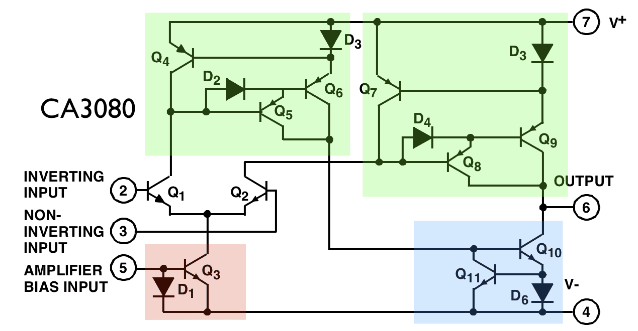
We can see there’s a Widlar mirror (in red) connected to pin 5. The two collectors of the differential pair Q1/2 are controlling two PNP Wilson mirrors (in green) like we’ve just looked at. The mirrors have been drawn with the PNP darlington transistor made explicit. Notice how the top-right mirror connected to Q2 is used to source current to the output pin, whereas the top-left mirror is used to control another mirror, this time a NPN Wilson mirror (in blue), which is used to sink current from the output pin. These two mirrors above and below the output pin therefore give it the ability to source or sink current as required.
The new Alfa Rpar clone, the AS3080E, is exactly the same as the CA3080, except that they’ve added the linearisation diodes (highlighted in red below) that the later LM13600/LM13700 chips introduced. This is the only difference. Since the original 8-pin package above only uses six of the pins, there are two left that aren’t connected (pins 1 and 8). They were able to use one of these for the diode bias input, which means that the chip remains entirely compatible with earlier circuits that use the CA3080, but offers an extra feature for modern circuits if you want it.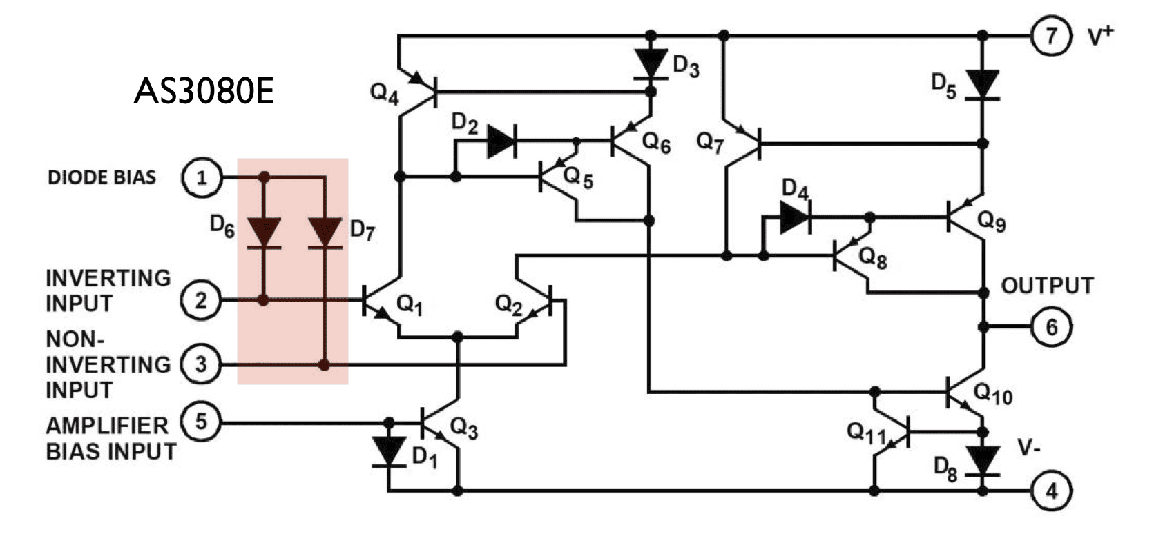
The LM13600 / LM13700
What about the LM13600? Here’s what a single OTA from the chip looks like: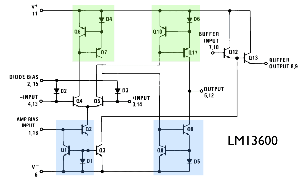
The overall layout is exactly the same as the CA3080. We have the same pair of PNP Wilson mirrors (in green) at the top, and the same NPN Wilson mirror (in blue) to sink output current in the bottom right. Notice that they’ve simplified the schematic and drawn the PNP darlington transistors as a simple single transistor. It’s important to note that internally this will be exactly the same as the CA3080. It’s only a question of how they’ve chosen to represent it on the schematic.
The most significant change from the CA3080 is in the bottom left. Instead of using a Widlar mirror to sink current from the differential pair, they’ve used another NPN Wilson mirror (in blue again). This is why the Amp Bias Input of the LM13600 and LM13700 is two diode-drops above -V and not only one diode-drop like the CA3080.
The other changes are the addition of a darlington buffer Q12/Q13 on the far-right along with Q3 to bias it, and the “pre-distortion diodes” D2 and D3 at the input. Since it is possible to ignore these parts of the chip and since they have no effect if they’re not connected, only the Amp Bias Input current mirror upgrade is significant when using the LM13x00 to replace the CA3080.
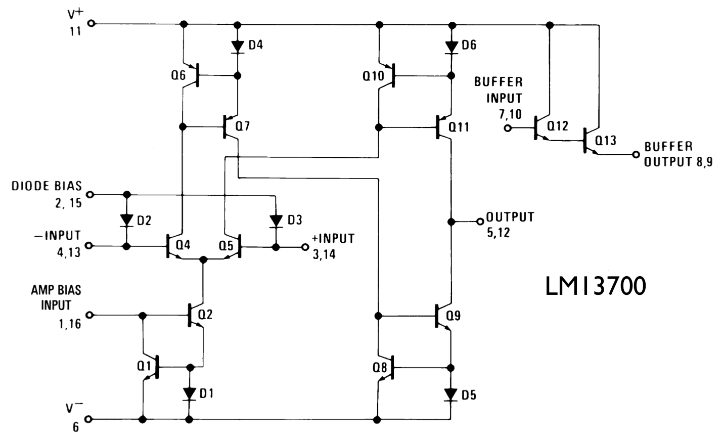
How does the LM13700 differ from the LM13600?
How does the LM13700 differ? Well, Q3 has disappeared! Notice also they didn’t renumber the other transistors, they did literally just eliminate Q3. There’s now no biasing shown for the darlington buffer at all. There must be something, but they’re not showing exactly what they’ve done instead.
The motivation for this change was to remove the buffer’s dependence on the Amp Bias Input current. This translates into less control feedthrough when using the darlington buffer.
If you’re not using the darlington buffer, the LM13600 and LM13700 are completely identical – totally interchangeable.
There’s one other device you might come across, which is the Alfa AS13704. This is a quad version of the 13700 OTA, but without the darlington buffers.
Summary of the differences between CA3080, AS3080E, LM13600, and LM13700
The differences are:
- The CA3080 and AS3080E use a simpler Widlar Mirror rather than a Wilson Mirror for the Amp Bias Input. This means that pin is one diode-drop above the negative supply in the CA3080/AS3080E, but two diode drops above in the LM13600/13700.
- The LM13600, LM13700 and AS3080E all include input linearisation diodes, if you want to use them.
- The LM13600 and LM13700 include a darlington buffer, if you want to use that. The buffer bias in the 13700 is arranged for less control feedthrough than on the 13600.
- The LM13600/LM13700 are dual OTAs, whereas the CA3080 and AS3080E are single OTAs!!
And that really is about it! They are all very similar, for sure, but they’re not identical.
Sources
- Eugene Zumchak’s article on Schmitzbits.de
- Achim Gratz’ paper on OTAs
- Intersil AN6668.1 Applications of the CA3080 OTA
Comments and Feedback
Please feel free to provide any feedback, error reports, or comments below!
Lovely article, thank you for it.
Not long ago I have bought reasonable amount of AK317D’s (for really good bargain) and looking at the diagram, they are pretty identical to 13700. Main difference, I had to get used to, was that it has different output current range and so, when for example I use it as current source for oscilator, I am getting different frequency range than when I used in same circuit with 13600/700. For VCA’s or for triangle to sine converter I find them fully interchangable sofar.
All the best!