
This voltage-controlled LFO is based on the PIC 16F684, which is a pretty basic chip. Nonetheless, this LFO has more features than your average LFO. For a start, it can produce 7 basic waveforms, and also includes a noise source. It can also morph its waveforms under CV control, well beyond basic PWM.

There is an optional sample-and-hold module that can sample whatever is selected, the current waveform or the noise source. The LFO frequency, waveform selection, waveform distortion, and S&H rate are all voltage-controlled using 0-5V. The overall output level is also voltage-controlled.
Block Diagram
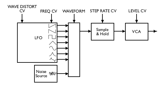
The chip uses the analogue inputs of the PIC for CVs. These are fed to the internal A/D convertor, which samples each input every 150uS or so and converts the voltage to an 8-bit value. In order to avoid using an external D/A convertor for the output, the chip uses the built-in PWM module. The PWM output needs passing through a lowpass filter to convert the pulses back into an analogue output.
Using an external crystal with the PIC allows the chip to run at its maximum clock speed of 20MHz, and this means that the PWM module is able to produce a 19.5KHz sample rate at 10-bit accuracy. I’ve tested the LFO by feeding the output into the filter modulation input of a SH101. No digital artifacts are audible on the straight-line waveforms (Ramps, Triangle, Square), but there is a slight stepping on the curved waveforms at the lowest frequencies. The SPIKE waveform is the worse case, since it has the steepest gradients. I’m considering adding interpolation to remove this slight problem.
Later note: I’ve gone back to the code and reduced this problem significantly by concentrating the lookup table on the steepest parts of the SPIKE waveform. Similar tricks have been applied on other waves too, and the errors have been reduced by 33% to 70%, with the best increase on the SPIKE wave.
Pinout Diagram

Waveform distortion

The WAVE DISTORT CV input can produce phase distortion of the LFO output. The waveform is regarded as being in two sections, usually half the total length of the waveform. By reducing the time one of these sections takes whilst increasing the time the other takes, it is possible to distort the waveform without altering its pitch.
More details
If you’d like to build one, or like to know how I built mine, perhaps you’d like to look at:
- Firmware Flowchart
- Voltage-controlled LFO PIC 16F684 ASM code
- Assembled HEX code from above file
- Circuit Diagram
- VCLFO datasheet (includes circuit diagram, example waveforms, and chip pinout)
By way of explanation of the flowchart, perhaps it is worth saying that the code consists of two main sections:- An interrupt routine that runs the LFO and noise source and ensures a constant output sample rate and frequency, and a main code loop that polls the various A/D channels (CV inputs) in turn and converts their values to something useful for the code. It’s also worth pointing out that I did the flowchart diagram before I added the WAVE DISTORT CV feature, so that doesn’t appear.
Update: Current Version 9D
The chip still had quite a few pins free, so I felt I could add some more features. A couple of things weren’t in the original version:
- The SYNC input that resets the LFO waveform or S&H back to the beginning.
- The WAVE DISTORT input to bend the LFO waves out of shape.
I’ve also reworked the PWM filter to use a two-stage 4th order Bessel filter. This improves the performance and reduces digital noise on the output. I hadn’t studied filters much before, and the existing design I chose to use originally was a Chebyshev filter which has a steeper rolloff, but not such good high frequency performance. For this application, the rolloff isn’t so important, but high frequency performance definitely is.
Update May 2017: New version VCLFO10
I’ve recently done a new version of this chip, taking advantage of the facilities offered by some of the newer enhanced PIC 16F processor chips. This has enabled me to add a second set of eight waveforms, improve waveform resolution to 16-bit, improved the sample rate to 31.25KHz, and remove the need to run the chip from an external crystal. All in all, the new chip is a massive improvement over the older one.
Full details and example schematics are in the VCLFO10 datasheet.
Have you considered an control to vary the PW of the square wave cycle?
Initially, that’s exactly what I had – a Pulse Width control which affected only the square wave. However, I was never happy with it because it didn’t do anything to the other waveforms. After a while, I came up with the Wave Distortion control, which still produces pulse width modulation on the square wave, but *also* alters the other waveforms too. So there still is a PW control, but now it’s labelled Wave Distort because it’s more general.
It still doesn’t alter the Noise output, but you can’t have everything!
I’d like to power the vclfo circuit from a single rail 5v supply. What is the minimum requirement to turn the PWM out into a useable waveform? Could you suggest a simple single rail circuit?
There’s a simple 3-stage passive filter in the LoopEnv datasheet, page 6:
https://electricdruid.net/datasheets/LOOPENV1Datasheet.pdf
That would do the job without any worries about the supply. Drop me a line if that doesn’t work for you.
Hi Tom. Great work!!! Thank you!
Just a quick question…can the SYNC IN pin accept higher than 5V voltages?
The official answer is “No, absolutely not”. In reality, the PIC’s input protection is pretty good and if you had a 4K7 in series with the pin to limit the current, you might get away with it. That’s the quick-and-dirty way. The much-better-engineering way is to put a transistor buffer in front of the pin to save the PIC from over-voltage or negative voltage. Something like this: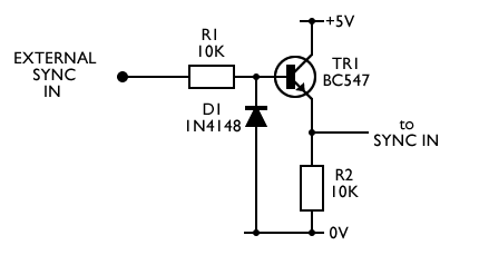
Incidentally, this is exactly the same circuit as I use on the Tap Tempo input of the TAPLFO, but using a pull-down resistor and the transistor pulling the level up to 5V instead of the the other way around. That’s because the TAPLFO expects short-to-ground inputs, not positive pulses like the VCLFO.
Thank you!!! Will try that
Does the freq cv control the noise pitch too?
No, I’m afraid it doesn’t, but you can use the Step Rate CV to controls how fast the noise is sampled for the Sample & Hold.
Tom
Hi Tom. What should i do with the sync in, sync mode and Sample and hold pins? Initially I want to set this up without an external sync control, just using the rate, wave-form and distortion controls. Many thanks,
Steve
If you’re not using the Sync In and Sync Mode CV pins, they should both be tied to ground, say with 10K. The PIC doesn’t like to have floating inputs. The Sample&Hold (“Step Rate CV”) is also disabled at 0V, so tie that to ground too.
HTH,
Tom
Thanks for your help Tom.
Best wishes,
Steve.
does the new chip get rid of the stepping completely?
Honestly, I don’t know. All I can say is that with the VCLFO10 I aimed to improve it in as many ways as I could. Where did you find stepping on the VCLFO 9D?
I mentioned above that I wondered about adding interpolation to help. Well, on the VCLFO10 I did add interpolation. And I also adding waveform smoothing as well. The only source of stepping now is the 10-bit limit of the PWM.
Tom
Dear Tom, sorry for the maybe stupid question – but could it be used as an oscillator? What is the range of the LFO? Cheers
The VCLFO 9D covers 0.05Hz to 25Hz. So it might work for sub-bass, but it’s not a typical VCO! You could have a look at the VCDO if you want something that produces audio frequencies.