
The LM13700 is a bonafide classic synth chip, plus it’s cheap and *still* available decades after it was originally introduced. Ok, it’s no longer the state of the art, and its noise and distortion figures are pretty poor, but that’s actually a part of its charm. It’s definitely got that “vintage sound”. So let’s have a look at how we’d actually use it. We’ll design a simple linear “Vintage VCA”.
A Eurorack VCA with the LM13700
Let’s assume we want +/-5V (10Vpp) input and output signals, and let’s design for a 0→5V control voltage (gain CV) level. The audio signal levels are pretty standard, but Eurorack envelope modules vary in the output level they provide. Doepfer’s original gear produces 0→8V, but many subsequent manufacturers have used either 0→5V or 0→10V. Consequently, designing for a low CV input level and providing an attenuator for larger envelope signals is a sensible course of action.
Firstly, we need to look at how much input voltage the chip needs. The short answer is “not much” because OTAs can only cope with very low input levels. We need the datasheet for the LM13700 OTA to tell us the detail. There’s a graph on page 6 that shows us what we need to know.
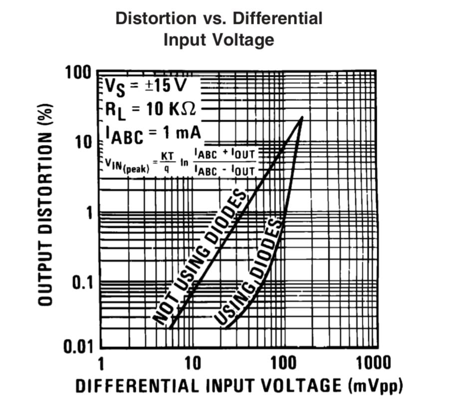
If you check the graph above, you’ll see that by the time the input signal level is up to around 100mV, distortion is somewhere between 1% and about 8%, depending on whether we’re using the linearisation diodes. Although there’s more distortion earlier if you don’t use them, I prefer the character of the chip without them. The approach to distortion is much gentler (shown as linear on the graph) and you get a “soft drive” sound rather than sudden hard clipping. If we’re not using the diodes, we probably better keep the input voltage well down under 100mV. 50 or 60mVpp give 2 to 3% distortion, so let’s go with that.
We’ve got 60mVpp as our maximum input, so we need to scale our 10Vpp input down.
10V / 60mV = 166.667

1 / 166.67 = 0.006
Our 10Vpp input is nearly 167 times too big! We need to reduce it to x0.006. A simple voltage divider on the input will do, and values of 100K/620R will provide the scaling we need.
R2 / R1 + R2 = 620R / (100K + 620R) = 0.006161

10V x 0.006161 = 61.6mV
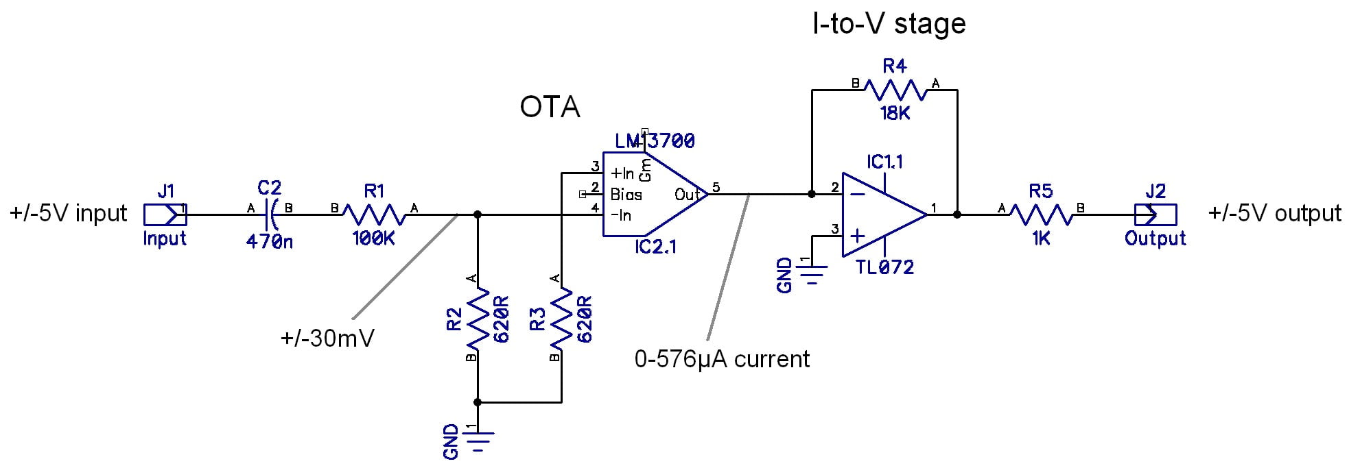
In highly-technical electronic engineering circles, this is known as “close enough” ;). So far, our circuit looks like this:
 Notice we use the same 620R resistor on the other (unused) input of the OTA. This helps minimise offset voltages. We feed our input to the inverting input of the OTA because the output will get flipped again later on. We’ll come to that.
Working out the output level of the LM13700
The LM13700 isn’t a simple op-amp. It’s an “Operational Transconductance Amplifier” or OTA. I’m going to avoid trying to explain what the hell that means. The short answer is it has an extra input that allows us to set the gain of the chip using a current. This control current is known as Iabc in the LM13700 datasheet, and the relationship between the input, the gain control current, and the output looks like this:
Iout = (q / 2kT) x Iabc x Vin
Ok, hold on! What on earth is all that lot?! Brace yourself…k is Boltzmann’s constant, T is temperature, and q is the charge of an electron. Yeah, seriously. Blame a physicist.
You also see kT/q referred to as the “thermal voltage”. The worst thing about it is that word “thermal” – it depends on the temperature – but if we assume room temperature, the thermal voltage is 26mV, and the whole mess simplifies:
kT / q = 26mV, so q / kT = 1/26mV

q / 2kT = 1 / (2 x 26mV) = 1 / 56mV = 19.2
That makes everything a lot easier. We can now write our input/output equation as:
Iout = 19.2 x Iabc x Vin
Iabc can have an absolute maximum of 2mA before the chip blows up. However, staying under the absolute maximum isn’t our only concern. The output offset voltage moves around as Iabc varies, and this translates into control voltage feedthrough from the gain input. To help minimise this, it makes sense to keep Iabc lower. Let’s design for a 500µA maximum control current. What’s our maximum output?
Iout = 19.2 x Iabc x Vin

Iout = 19.2 x 500µA x 60mV = 576µA
The output from the chip is not a voltage, but is a current instead, hence Iout not Vout.
Converting the LM13700’s output current to voltage
In cheap’n’cheerful 13700 circuits, you’ll often see a resistor hanging off the output down to ground. This resistor acts to take this current to ground, and if a current is following through a resistor, there must be a voltage across it, so the resistor converts the current to a voltage. Here’s an example from the datasheet. I don’t hold with such disgraceful practices. Ok, not often.
There is a active circuit that does the same thing with somewhat better performance, a building-block op-amp stage known as an “I-to-V convertor”, or sometimes a “transimpedance convertor”.

The I-to-V stage looks a lot like an inverting op-amp with the input resistor chopped off, and that is basically what it is. It gives an output voltage which depends on the input current Iin and the feedback resistor Rf.
Vout = -Iin x Rf
Notice that if you *increase* the feedback resistor, the output voltage goes up. This is like the inverting op-amp, where increasing the feedback resistor boosts the gain. Also notice that negative sign; like the inverting op-amp, this circuit inverts the output.
Since we know what the current is from the OTA, we can work out what resistor we need to get our required output voltage:
Rf = Vout / Iin = 10V / 576µA = 17.36K
The nearest practical value is 18K. So now our VCA circuit looks like this:
Turning a 0-5V CV input into a safe Iabc control current for the LM13700
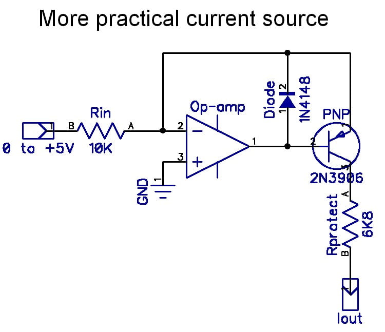
We’ve just looked at turning a current into a voltage, but for this part of the circuit, we want to turn a voltage into a current instead. The same thing in reverse! There are lots of current source circuits you could use. We’ll choose this one:

This is a good design because it’s simple and nice and linear, which is what we want for our VCA. The input resistor goes to a virtual earth node at the inverting input of the op-amp, so we can add further input resistors and mix them together without them interacting. That’s very handy. It’s also very easy to work out Iout, since it’s the same as the current through Rin.
There are various ways you can think about how this works, but one way of looking at it is the following: Since the inverting input is infinite impedance, no current can flow into it. Thus the current coming in through Rin must be matched by an equal and opposite current provided by feedback from the transistor. Since the direction of the input current is into the inverting input, the direction of the feedback current must be out of the inverting input, and into the PNP’s emitter. Since the op-amp will try and hold inputs at the same voltage (ground, as pin 3 is grounded) then the output will drive the transistor base as negative as is required (it’s a PNP, remember) to develop the required feedback current through the transistor.
Iout = Vin / Rin
We want 500µA, and we wanted to use a 5V level, so if we re-arrange the equation to find the resistor we need:
Rin = Vin / Iout = 5V / 500µA = 10K
So we just need a 10K input resistor. Of course, things won’t stay that simple for long. This is very much a “textbook” circuit, which is to say, it’s an idealisation, and it doesn’t include several components we will need in a practical circuit. Firstly, it would be a good idea to add some protection for the Iabc input of the LM13700 just in case something goes wrong. The worse case scenario would be a short to one of the rails, so 12V. We’ve already mentioned that Iabc can only go to 2mA before the smoke comes out.
R = V / I = 12V / 2mA = 6K
We can use 6K8 to be on the safe side. We also need to think about negative voltages. The circuit won’t provide any output if the input voltage goes negative since the transistor will be switched off. But it will also be reverse-biased, and eventually that will fry it. If we add a diode from the base back to the input, we provide an easy path for the current to take that avoids the PN junction inside the transistor (that’s what that little arrow in the symbol represents). So now we’ve got this:
This circuit above will work, but it’s still pretty basic. We’ve only got a single input, and we haven’t got any kind of manual control for the gain. We could naively tack a load of stuff on:
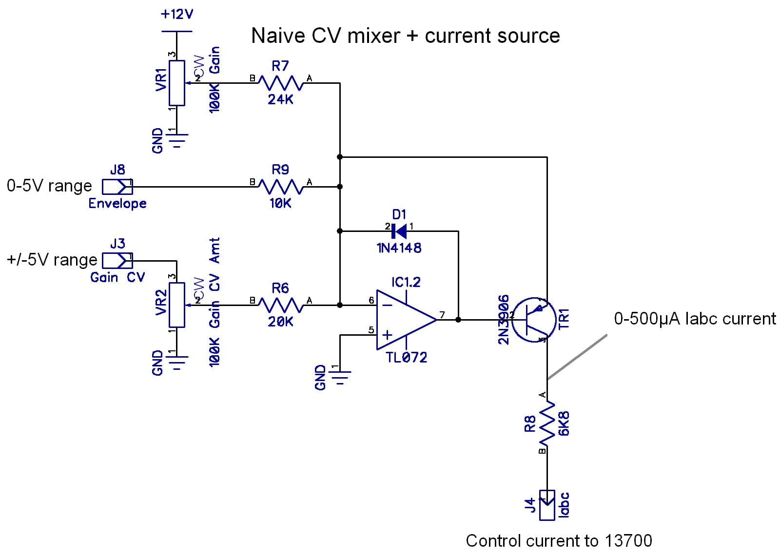
Ok, so what have we got here? Our 0-5V CV input is still there, marked “Envelope” in the middle. Above it we’ve got a manual gain control pot which provides 0-12V. Since this is a larger voltage, we scale up the input resistor appropriately. At the bottom we’ve got a general purpose CV input set up for a +/-5V range. This has the standard 100K attenuator pot, and the 10V range means we need to double the input resistor to 20K.
So what’s the problem? Well, if we try this circuit, we don’t get the voltages or currents we expect. They’re all rather low. This is because we’ve forgotten to think about the input impedances. Take the +/-5V Gain CV input, for example.
20K is a low input impedance, and becomes even lower since it is effectively in parallel with the lower half of the CV Amount pot. The output impedance of whatever our CV source is might be low, but then we’ve got the upper half of the CV amount pot in series with it, so it could easily finishes up being 50K or so. The result of all this is the input presents a significant loading and we lose some of our CV signal (about 10%) and we also badly deform the pots response curve, so a linear attenuator pot no longer behaves in a linear manner.
In order to avoid this effect, the general rule of thumb is to make input resistors ten times larger than pot values. This doesn’t stop them from being in parallel, but when a “large” resistor is in parallel with a “small” resistor, the value of the parallel combination is basically the same as the small resistor.
With a 100K pot, going up to ten times the value for the input resistor is a bit large (1M), but we could manage 470K without pushing things too far, and checking the situation in a simulation shows us that even 330K is almost linear. But wait! If we alter the input resistor, we alter the amount of current we get out of our circuit. We have to compensate somewhere else. Luckily the solution is provided by the bible of synth builders, Hal Chamberlin’s book “Musical Applications of Microprocessors”. Turn to page 203 (2nd edition) where he presents an even-more-vintage VCA design using the CA3080:
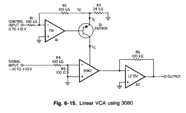
See those extra resistors at the top? R2 and R3? They split the feedback current from the transistor and effectively allow us to set the gain of the current source. Like this, we can use whatever size input resistors we like, and then scale the output current back up using a bit of gain in the current source. This gives us a schematic for our final current source:
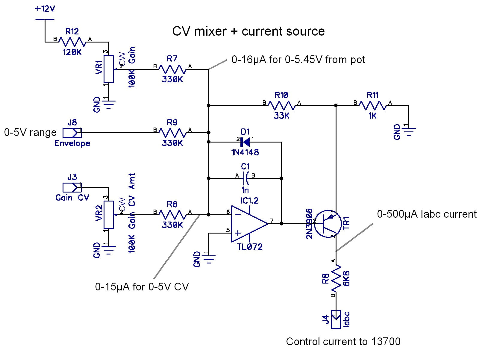
And that pretty much wraps up our Eurorack VCA design! The only other thing I haven’t mentioned is the addition of C1 which works in tandem with R10 to add some smoothing to the CVs and keep some noise out of the CV path. The whole thing looks like this:
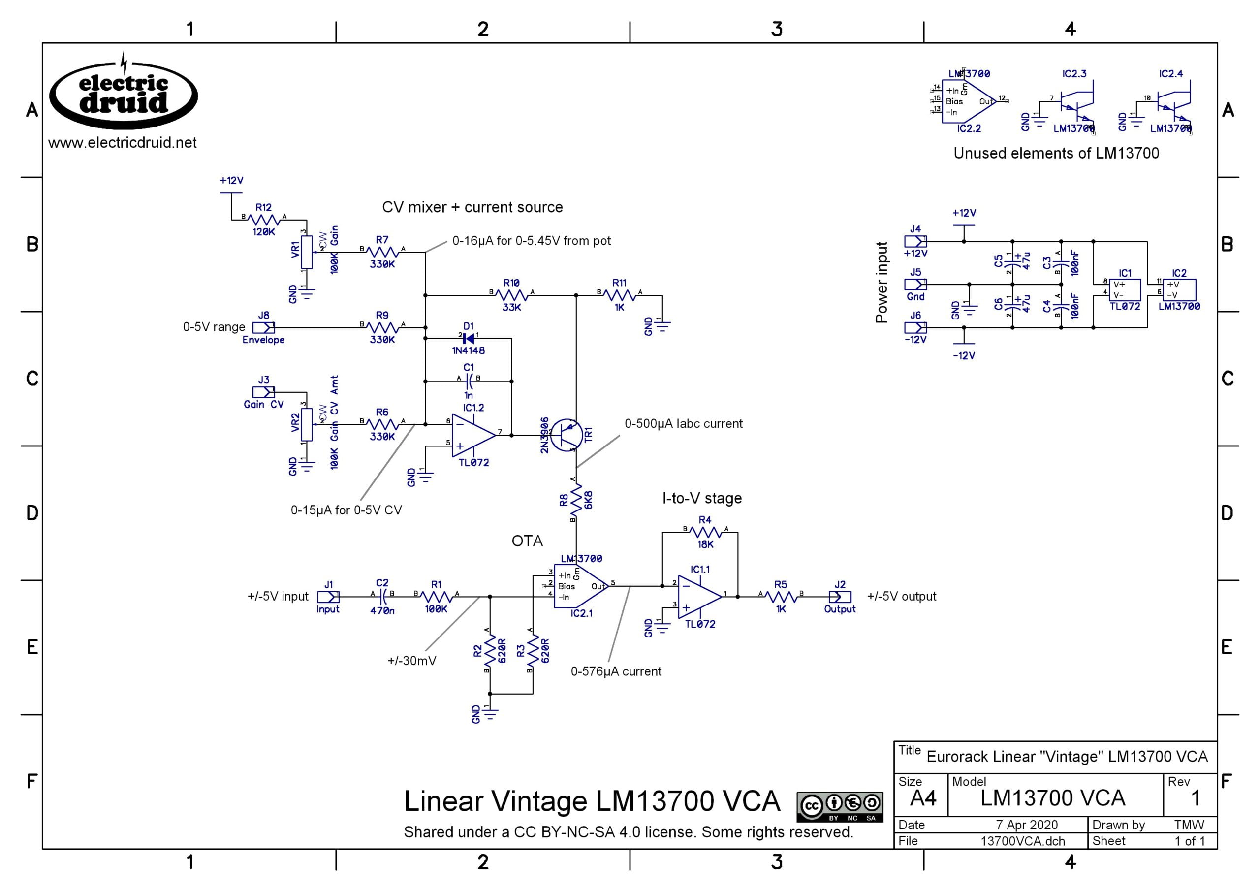
It might make sense to build this as a dual unit, since there’s another VCA in the LM13700 that we’re not using. Building two of these on the same PCB would save wasting one VCA. And anyway, you can never have too many VCAs, right?!?
Further reading on the LM13700
For a lot of extra detail, you can’t beat this excellent paper.
“Minimizing Distortion in Operational Transconductance Amplifiers”, Open Music Labs
There’s also this classic article on the LM13700, if you haven’t seen it.
“Understanding and Using OTA op-amp ICs (Part 2)”, Ray Marston
Comments and Feedback
As usual, if you spot any errors, get in touch, or comment below.
Thanks so much for this terrific article!
If the VCA is not closing all the way, what would be the best way to correct this?
My first instinct was to connect a 3M resistor to -12v at the CV mixing input stage. This worked, but I feel like maybe it chops off the end of the incoming envelope a bit? Not sure. Are there better ways to make sure a VCA closes?
Thanks Colin.
The principle of connecting a little bit of negative voltage into that mixer is good, so your -12V via 3M is working, but it sounds like it’s still a bit too much if it’s cutting off the end of the envelope. How about trying a trimmer pot between ground and -12V and then take the wiper output via 1M/2M2 to the mixer or something? That’d let you dial it down to “just enough” a bit better.
Another alternative solution would be to connect the bottom of the gain pot VR1 to a 200K resistor to -12V, instead of directly to ground. That would allow the pot to go slightly negative and give you a panel adjustment for the offset.
Let us know how you get on!
Thank you for the very nice explanation of this circuit! i would love to read more “step by step” articles about the common eurorack circuits as i’m still learning more complex circuit designs.
Thank you for this! It has helped me a ton! I have a question regarding the examples from “Musical Applications of Microprocessors”
“See those extra resistors at the top? R2 and R3? They split the feedback current from the transistor and effectively allow us to set the gain of the current source.”
From reading that section in the book, I understand that R2 and R3 form a parallel resistor. But I’m confused about the formula to calculate the current gain. What is the formula for getting 500microamps from the 15microamps in your example? Thank you!
We know that the current through R10/33K must be 15uA because it has to carry the 15uA that comes in through R6. If R10 and R11 are in parallel, then the current flowing into them will split proportionally according to their values. So if R11 is 33 times smaller than R10, it must carry 33 times the current. That gives us 15uA x 33 = 495uA. So the total current from the transistor is 15+495 = 510uA. The control current will be slightly less since we lose a bit to the transistor base, so we can say that the collector current is “about 500uA”.
Just built this and it works perfectly with my Doepfer set-up, nice one!
Hi Tom,
I see some OTA VCA designs that have a pot wired to plus and minus voltage as an initial on level. Presumably this works with the CV mixer so you can use an LFO as a CV source. How would this work with the design here with the diode in the CV mixers op amp feedback path? Is there a chance of burning up the transistor still?
Having the initial level pot across +ve and -ve voltage just gives you a bit more flexibility about offsets. If it can go negative too, you can cancel a positive offset on the CV input and get the VCA to go properly ‘Off’. Whether that’s a likely enough situation to warrant using half your knob travel is a matter of taste! (An LFO would need a positive offset to shift it up above zero).
The diode is still required, since the current to the VCA itself has to stay within range, no matter what CV inputs we throw at it.
Thanks Tom. I will have to play with that. I’m thinking of using an inverted envelope in the CV so being able to offset positive would be good as well as using LFOs as a CV source.
If I were to make this a stereo VCA, how would you suggest I go about that? I imagine I can’t just splice off the bottom half of R8, as I’d get half current. If I changed the values so it put out 0-1.1mA, I worry that the VCA’s could ‘take in’ uneven amounts of current for the gain, so I would end up with unbalanced levels.
I’ve just got the single 0-5v range input on my design, no CV input.
I’m thinking I could just add another transistor (and assosciated R10+R11 divider) to pin 7 of the opamp, and having two seperate current outputs?
Or is none of this going to work, so I should just use another op-amp and split off the 0-5v envelope input, and create another current source block?
Personally, I’d try the simple way first – just connect the two Iabc inputs together. I’ve certainly seen other 13700 circuits that do this, so it’s not impossible. The two OTAs on a chip should be well matched (same bit of silicon, after all) so I doubt one would draw significantly more current than the other.
Good luck, and let us know how you get on!
Thanks Tom 🙂
Made some tweaks for my application – I don’t need gain control or the -/+ 5V range, so I’m just using the “more practical current source”. Doubled the current (as each VCA module will use half the current), using 5K1 instead of 10K as Rin.
And just connected the two Iabc together and it worked without a hitch!
Thanks for the great article, really helped me understand the calculations and design!
Glad to hear you got it running, and glad you found the article useful.
Can you further explain the purpose of R3 going into the positive terminal of the OTA? Why do you not just put the voltage divider straight to ground across the OTA without that second 620R resistor? How does it minimize offset voltages? Thanks for the great writeup!
You could use just the voltage divider without the second 620R resistor. It would work fine. The second 620R is just good practice, rather than essential. It minimises offsets because it helps balance the effect of bias currents at the two inputs. If the two inputs see totally different resistances, the bias current will cause a different voltage drop across those resistors, and that difference shows up as an offset. The theory is that you should use R3 = R1||R2 (in parallel), but in this case, that’s roughly R3 = R2, because R2 is so much smaller than R1.
In practice, there’s probably a significant offset anyway, even without the bias current effects, which is why you often see these OTA VCA circuits with a little trimmer attached to one of the inputs to trim it out. I left that out, but you could add it if it was important.
Thanks for the writeup, this has been really helpful to understand how to design with OTA’s. In the intro you mention varying voltage standards for the envelope input (0-5V or 0-10V) that can be addressed by attenuating the input. Is this omitted deliberately on the Envelope input, or expected to only be used with the Gain CV input?
It’s an example circuit, so the two different inputs are examples of two different approaches is all. If you need input attenuators, you can add more inputs like the Gain CV example. If you needed 0-10V or 0-8V input only, I hope there’s enough information given to show you how to work out sensible values for the resistors.
Why is it when you went from the naive inputs with low impedance to the final version, the input resistors that were in a ratio of 10:12:20 became all equal?
It’s because I changed some other things too, to ensure that all those input resistors could be high impedance. The Gain CV input which was set up for +/-5V (so 10Vpp) is now scaled for 5Vpp. OF course, you can still feed 10Vpp into it, but you’d have to turn the input pot down. That’s what it’s for after all. And for the VR1 Gain control at the top, I added a resistor above the pot to limit the voltage instead of scaling the input resistor. In that case, that’s not the only choice. We could have kept the pot going to 12V and used an 800K input resistor (ok, it’d be 820K – close enough). Since 800K isn’t going to load the pot, that’s fine too.
hi Tom, great article!
for the possibility of AC/DC coupled input, could you just bypass C2 with using SPDT switch for example?
like in VCA-1 from Thomas Henry? https://www.birthofasynth.com/Thomas_Henry/Pages/VCA-1.html#VCA-1_Documentation
cheers!
Yes, I don’t see why not. It wasn’t designed with DC operation specifically in mind, so it might need the odd tweak, but it should *work* at least.
hey Tom, thanks a lot for the great article!
there’s a thing that I can’t wrap my head around, I hope you can help. if I get it right, in order to have 500uA as Iabc the TR1 should be in the active region, ie. Ve > Vb > Vc. from which Ve > Vb is true, since Ve is on the virtual ground potential and Vb Vc)? sorry if it’s a dumb question, I’m new in electronics
hm… my original question was cut for some reason :/
anyways, what I don’t get is how will the collector voltage be smaller than the base voltage so that the transistor is in its active region? thanks a lot
For the PNP transistor to turn on, the base has to be more negative than the emitter. That’s not difficult for the op-amp to achieve, since the emitter is tied to a virtual ground node, so 0V. The op-amp output can drive the base anywhere between the rails, so depending on the op-amp, that would likely be +/-10V or more on a +/-12V supply.
PS: Your original question wasn’t cut, just waiting for moderation.
thanks for the answer Tom! I understand the base emitter relation, but shouldn’t also the collector be more negative than the base to be in the active region?maybe I’m missing something obvious.
The collector in this circuit is tied to the LM13700 Iabc input, which is two diode drops above the negative supply, so that works pretty well, I guess. That gives the op-amp plenty of room between 0V and (-12V + (2 x 0.7V)) = -10.6V to adjust the base and have it more negative than the emitter and the collector more negative than that.
To be honest, I hadn’t thought about this aspect at all.
nice! in the meantime I did further research and found what you’re saying in the datasheet of the LM13700 too (page 12. last paragraph) and also in Musical Application of Microcontrollers: “The control current is fed into the Ie terminal and is absorbed at a constant voltage of about – 14.4 when using 15-V supplies.”. thanks again for helping, now I understand the whole thing 🙂
I´ve done some adjustments to get dead silence out of this circuit.
I´m no professional, but at the end it gives me a better result.
R2 & R3 590 ohm
R7 & R9 & R6 220k
Gain Pot Pin 1 through series 180k to -12V
9,2Vpp output.
In case you don´t have 470n caps around for the input, i´m using 100nF ceramic. i guess a 470n film would be best here.
For me it´s more important to have a silent VCA than precise 10Vpp. Eurorack levels are hot enough to compensate this marginal loss of 0,8Vpp.
I´m sure this can be optimized with fiddling the super sensitive input resistors of the OTA and the resistors around the gain pot. For stereo use match all resistors and transistors, buffer the cv ins and give switch or optional jack for feeding both VCAs.
I have to do some corrections,
with the mentioned values i´m experiencing a little deadzone in the first 10% of the gain stage.
It seems like i´m having the perfect balance now.
I´m attaching a falstad link in case you guys want to check the simulation and in case Tom is allowing this …
The values i´m having now:
R7, R9, R6 – 270k
R12 – 100k
R3, R2 – 590R
Gain Pot Pin 1 through 180k to -12V
Output Level 9,6Vpp
The Simulation will explain itself. It´s including manual gain control and an envelope with attenuation.
OTA VCA circuit in Falstad
Thanks!
Changing R2/R3 only affects the input level, so it’ll change the potential distortion you get with a given signal level but shouldn’t affect the ‘off’ state.
Someone else mentioned that they couldn’t get it to go completely to silence. Like you’ve done, the solution is to allow the gain pot to go slightly negative to counteract any positive offset there might be.
Hi Tom — Thanks so much for this article, and the related one on the single VCA cross-fader ( https://electricdruid.net/single-vca-crossfader/ ). Very nicely done. They clarified several issues for me and are a big help for phaser which I’m trying to design with some voltage controlled elements. I’m a professional physicist and a hobbyist with electronics. As such, I’m willing to accept a portion of blame for the q/kT thing. Actually, before I get into my questions I have a comment to add about that which might be of interest to your readers. A core property of diodes (NP junctions, as doubled up back-to-back in a transistor) is exponential current dependence on voltage. The argument of an exponential function must always be dimensionless (no units) … otherwise relations like e^x = 1 + x + x^2/2 + … wouldn’t make any sense. So, they must reference a *ratio* of voltages to cancel units. The problem under consideration then has to supply a reference voltage scale for comparison that is built strictly out of constants of nature and parameters directly relevant to the problem . Boltzmann’s constant just turns temperatures (in Kelvins) into an energy kT. Also charge times voltage qV is an energy. So, kT/q will be a scale value in units of volts — it pretty much “has to” make an appearance for those reasons, because there’s nothing else you can build with the right units. This is analogous to the way in which R and C combine to give a time constant for filters, or the drag parameter, mass, and gravitational acceleration g combine to give the terminal velocity of a falling object.
In my application, I am limited to a single-sided supply, let’s call it 0 to 10V. Accordingly, it should be possible to shift and rescale all the external voltages in your example for the current source feeding I_abc. But, I also need the control voltage to stay pinned at 0 to 5V. I think I have finally realized how to do this, but let me walk through the thought process and problems I was having getting there. With the op-amp supply voltages at 0 and 10V, all the grounded locations in your diagram should be shifted to the midpoint, a 5V reference. If I am understanding correctly, the whole point of attaching control voltages to the inverting input of the op-amp is that continuity of current (and the high input impedance of the op-amp) implies that the transistor has to replicate the value of that input current, while buffering and decoupling it. It also provides in a nice way for summing if need be. But, since I_abc must be positive for operation of the LM13700, the 0-5V input control voltage is unsuitable, since it would yield a negative current flow relative to the 5V reference on the non-inverting input. The fix seems to be attaching a fixed 10V potential to the inverting input, in parallel with the 0-5V CV, and across a matched resistance. Then, the input current will always be positive, going to zero when the CV is 0 (currents driven by the 0-5 = -5V and 10-5 = +5V legs sum to zero).
I’m curious whether that sounds on target to you, or if there would be different advice? Thanks much, Joel
Hi Joel,
Thanks for the interesting remarks about q/kT and the physical basis for these units. I’d never have come at it from that angle, so that’s a view into a different world.
I’m not entirely clear what you’re proposing with the single-supply version of the circuit, but the main gotcha to watch out for with a single supply is that the op-amp in the current source won’t be able to cope if its input goes close to the rails. So 0-5V input gets tricky with 0-10V supply, because the op-amp probably won’t like having its input and/or output at ground. If your addition of a reference voltage prevents that, then I think it should be fine.
Thanks, Tom — I’m very pleased the comments were interesting. Thanks very much for the “gotcha” warning regarding the rails … that’s exactly the sort of real-world practicality that I’m prone to overlook as an amateur, and I will give it some additional thought.
Hi Tom — I have a follow-up to the prior which involves the possibility of replacing the LM13700 with a CA3280 (or actually the equivalent AS3280, which is in current production). I’ve done quite a bit of reading about these operational-transconductance amps. Transconductances and current sources are much less familiar to me than traditional impedances and voltage sources, and my intuition is limited. My impression is that the CA3280 is considered an upgrade to the LM13700 due to lower noise. But, it seems to also have quite a bit of additional circuitry related to current mirrors on the inputs for the I_abc gain control and the I_diode bias. My question is whether this additional circuitry essentially implies that the rather brilliant current source you described in the article becomes redundant when using a 3280 chip. In other words, is the current source buffering and stabilization being performed *in* the chip in such a way that one should feel comfortable just driving I_abc &/or I_diode with a simple voltage through a resistor, without any concerns about loading down that voltage? Even if that is partially true, are there other reasons to keep the current source that I’m not thinking of? I really like the design of that circuit element, but fewer parts is always better, all else being equal. Incidentally, I’m unable to find a spice model for the 3280 which seems trustworthy — any advice there? Thanks very much! Joel
My understanding was that the CA3280 was improved by using a better design for the current sources on the chip, giving lower noise and less distortion. I didn’t think it changed the behaviour of the Iabc input, but I’ve not really used the ‘3280 so I haven’t got any practical experience with it. Check the datasheet for the Iabc range, because it’s probably different.
OK, will do .. thanks!
Hi Tom,
finally got round to building this for my +/-5V synth box. Works a treat! The input summing resisters were a challenge but I was able to make them with two resistors to give the values I needed. The output from my AR generator (based on the Thomas Henry 555 design on Electromusic.com) outputs just over 4V so I calculated for that as max and changed the value of R12. My LFO gives just 4V on the square wave but about a lot less on the triangle so I made a voltage divider to bring the square down to that level and calculated the summing resistor accordingly.
The thing doesn’t shut up at ground but does at around -0.4V so a resistor from -5V to the gain pot gave that. As you said I didn’t need to run the pot from positive and negative.
Learned a lot from your article and a lot from building it.
Cheers
Jim.
Thanks for a great article.
Just a small note, Amp bias input is 2 diodes from the negative rail thus if you put 12V at the collector you get ~ 3mA through R8 (22,8V/6,8k) which exceeds maximum rating.
Hi Thomas,
Yes, thinking about it now, I think you’re right! That 6K8 would therefore need to be 22.8V/0.002 = 11400 = 12K.
Thanks for spotting this.
Tom
Hi,
Is it possible to adapt the circuit to make it work in a stombox format, using a stompLFO chip ? (the LM13700 powered with +9V DC power and a Vref at 4,5V instead of ground in the schematic)
It’s possible, but it’s not straightforward. The 0-5V StompLFO output needs shifting away from ground (because otherwise the op-amps will clip). But since the LM13700 needs Iabc to be two diode drops above the negative rail, we’d probably finish up doing that anyway.
Hello Tom. I’m trying the current source but it looks like R11 resistor doesn’t have any effect on the current amplification. with MM in current mode in series to ground (hooked to R8, to monitor Iabc), i read around 0-24uA.
Of course if i increase R10 (until around 300k), i get the range 0-500uA.
I think R11 should have an impact on the reading.. If i change its value the current should change proportionally, isn’it?
First at all thanks for the article and thanks for any hint.
The trouble is the multimeter measurement. Break the connection from R8 to the LM13700 Iabc input, and then connect the meter between the two. The Iabc input isn’t at ground (actually two diode-drops above the -ve rail) so it changes things a lot.
Yes, the R11 value should affect the reading proportionally, as you said.
Thanks so much for the clear explanation and great design. I built a dual version on pref board and it worked perfectly from the start- now living happily in my modular setup.
Stupid idea:
If you just want the 0-5v cv in and nothing else. You could you just run the tl072 from gnd to +5v, feed cv with 10k into -IN and a 6k8 on out into the OTA current source?
Something simple like this would work, but you’d need to use a rail-to-rail op-amp that can run at 5V. The TL072 isn’t suitable for that job. Its output can’t get that close to the supply rails (like 1-1.2V or so) so even if it did run on a 5V supply, you’d lose over 2V on the output!
Hey Tom. Thank you for taking the time to write this! I’ve been referencing it for the past few weeks with a circuit I’m currently working on. I’ve run into strange non-linear traits with the voltage-to-current converter/PNP section. When using it to attenuate the VCA, the VCA output seems to jump in amplitude when going from a CV input of 0v to 1v. On a scope it looks a bit like the forward voltage curve of a diode, when I’m supplying a 5v signal to the “audio” input of the VCA. It’s exponential – once I pass a certain voltage (likely around .7v) the amplitude shoots up and then becomes linear as I increase the signal beyond 1v. I haven’t found a way around this and was wondering if this is something you’ve seen before. Thankyou!
Are you running the circuit on a bipolar supply?
Yes, +/-12V
I can also provide circuit and o-scope photos if you provide a place to send them!
Ah-ha! I was using to large of a value for C1 (10nF).
Hello
I have a few questions about this circuit and the chip if you can please help.
Firstly I’m wondering if you can substitute the LM13700 with an LM13600? If the circuit will still work
And I can’t figure out from the image, its obscured witch is the correct input pin for the labc from the transistor and r8 on the ic??
I’m confused which pin it is supposed to come in on?
Thanks
Alex
Yes, the LM13600 should work. If I remember correctly, the differences are only in the darlington buffer section, and we don’t use that here.
The Iabc inputs are pin 1 or pin 16 (marked “Gm” on the schematic), depending which half of the chip you’re using.
Hi Tom
Thanks for clarification on that, its a big help thank you, I will give it a go with the 13600 then see how things go.
Thanks again!
“The Synth builders bible, Hal Chamberlain’s-Musical Applications of Microprocessors”
My thoughts exactly! 😁
Great stuff. Thank you. The 13700 and its forerunner, the 13600, were chips I could never get to work properly back in the day. All my VCA implementations fell back on NE570 parts.
Really dumb question. What are you good people using to power these circuits? Is there a decent +/-5V unit off the shelf? Amazon/RS/Farnell/Arrow? Would prefer to spend the time inhaling solder smoke on something novel.
Thanks for listening.
Hi,
thank you for that really good explanations! Do you think it is easily (without extra opamp) possible to add an optional logarithmic control input?
best,
Florian
I think you’d probably need an op-amp. You certainly need a transistor or two. The Thomas Henry VCF design is about as simple as you can make it. This filter is based on the CA3080, but Thomas says you can drop-in the LM13700, so you could use the control part directly:
https://www.birthofasynth.com/Thomas_Henry/Pages/VCF-1.html
Thank you for replying so fast = ) I am wondering if it is possible to integrate the circuit you mentioned
https://www.birthofasynth.com/Thomas_Henry/pdf/VCF-1/Sheet_0001.pdf
into your cv summing circuit. Or would it be necessary to convert the output current of your linear cv summing mixer into a (0-5V) voltage again which is then fed into the circuit of thomas henry which will then generate its own control current ? So in the end it is 3 op amps?
So using a switch it might be possible to connect the LM13700 of the VCA to either the linear or the exponential version? I am wondering if the linearily converted output current of your circuit will still be available when having the other current to voltage converter attached to it.
I tryed to create the schematic from the combined circuits:
https://platz.uber.space/share/wiltshire-vca-log-mod.jpg
Do you think that might work? Is there any chance to reduce the number of op amps used?
Thank you for your help!
You should be able to do it with one op-amp for the CV input mixer, followed by one op-amp for the linear current source, and one for the log current source – so three op-amps. But you’ll have to think about the levels at each point and tweak a lot of values because the existing schematics are assuming different things.
But do you think it would also work like this “wasting” the extra opamps for not having to think about complicated things?
https://platz.uber.space/share/wiltshire-vca-log-mod.jpg
Yes, in principle I don’t see why that shouldn’t work. It’s just messy is all!
Hey Tom,
I really appreciate this build walk through, it really helps to start understanding how each part of the circuit works.
I put it together on a breadboard and it’s working well. But in my circuit the response to the envelope is a little slow. For instance, when the attack is 0, the volume still has a small but noticeable ramp.
Thanks!
-Chris
Hi Chris,
Glad you’ve found the article useful. I don’t see much reason why it should be slow to respond. Are you sure the problem is the VCA and not the envelope itself? How fast is the fastest attack time? Does the VCA still have this “noticeable ramp” if you use a Gate signal to open and close it? (which should have a more-or-less instant attack/release).
One more thought, Chris: Have you got the correct value for R1 in the current source? That cap adds a bit of smoothing to the CVs to help filter noise. If it’s too big, it’ll act to slow down CV changes. So check that you’ve not got 100n in there instead of 1n. And if you have got 1n, experiment with taking it out and see if that fixes your problem.
HTH
Thanks for a great article! I successfully built a VCA based on this. However, I now realize that I would like to have an indicator LED showing the gain level, i.e. the voltage fed into IC1.2. Any suggestions how the circuit can be extended to include such an indicator LED?
Regards,
Karl